Image: Samsung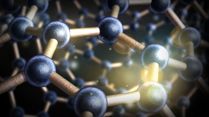
Researchers at the Samsung Advanced Institute of Technology (SAIT) have unveiled the discovery of a new material, called amorphous boron nitride (a-BN), in collaboration with Ulsan National Institute of Science and Technology (UNIST) and the University of Cambridge. Published in the journal Nature, the study has the potential to accelerate the advent of the next generation of semiconductors.
2D Materials – The Key to Overcoming Scalability Challenges
Recently, SAIT has been working on the research and development of two-dimensional (2D) materials – crystalline materials with a single layer of atoms. Specifically, the institute has been working on the research and development of graphene, and has achieved groundbreaking research outcomes in this area such as the development of a new graphene transistor as well as a novel method of producing large-area...
Continue reading...